
Inspiration
Full credit to WillsBuilds on YouTube, who built a stunning 8-inch magnetic ISS tracker that really sparked the idea. His build is beautiful — we highly recommend watching it.
The Orbigator set out to solve two specific limitations of that design:
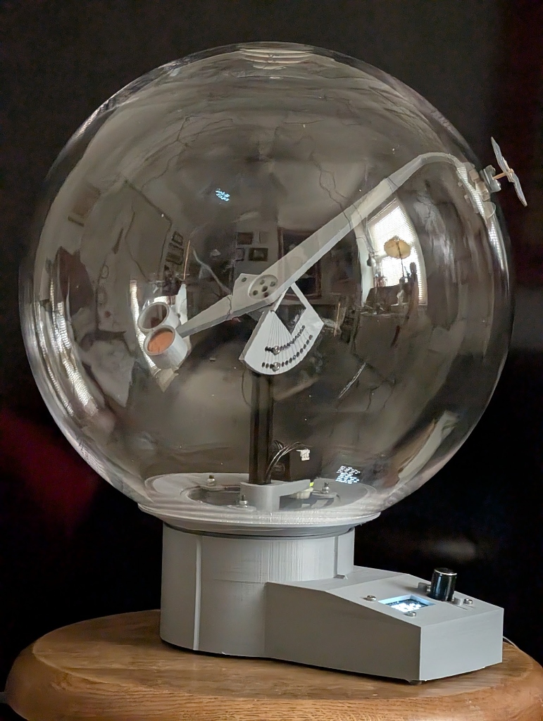
- The globe rotates around the mechanics. The key design inversion: rather than an arm pointing out from fixed electronics, the Orbigator puts the two-axis gimbal inside the acrylic globe, and the globe itself turns on the EQX (azimuth) axis as part of the mechanism. The sphere is simultaneously the display and the tracker — no cable fighting rotation.
- Continuous tracking, no rewind. Because the globe turns continuously with the satellite, the arm never needs to reset or skip. The ISS orbits indefinitely and the Orbigator follows every pass without interruption.
The Orbigator is a kinetic art piece and precision instrument — a two-axis servo-driven arm inside a 30 cm acrylic globe that points continuously at the International Space Station (or any tracked satellite) using real-time SGP4 orbital propagation.

How It Works
A Raspberry Pi Pico 2W runs a full SGP4 orbital propagator in MicroPython. Every second it fetches the current satellite position using a cached Two-Line Element (TLE) set downloaded from CelesTrak. The result — inclination angle and right-ascension angle — is sent to a pair of Dynamixel XL330 servo motors via RS-485, driving a two-axis gimbal arm inside the globe to point directly at the satellite.
- Motors: Dynamixel XL330 × 2 (Extended Position Mode, 1° resolution)
- MCU: Raspberry Pi Pico 2W (MicroPython)
- Display: 128×64 SH1106 OLED
- RTC: DS3232 with battery-backed SRAM for state persistence across power cycles
- TLE source: CelesTrak, auto-refreshed every 12 hours over WiFi
Overhead Alert Radar — New Feature
The latest firmware addition wakes the OLED display automatically when the tracked satellite rises above your local horizon. Rather than waiting for a scheduled pass, the Orbigator continuously runs a trig-free dot-product horizon test on every tracking tick (six multiplies and three adds — no atan2, no sqrt). When the satellite crosses zero elevation, a three-second dwell confirms it’s a real rise rather than a noise event, and the display wakes showing a radar-style sky plot:
- Left panel: Az and El in degrees, updated every second
- Right panel: Radar circle (horizon = outer ring, zenith = centre) with the satellite’s trail arc and a current-position dot
- The trail records one point per minute, covering the full pass from rise to set
- The display stays on for the entire pass, then returns to normal idle-timeout behaviour
Observer location is determined automatically at boot by querying the Wyolum geolocation endpoint, which returns latitude and longitude based on the device’s public IP. The ECEF station position and local East/North/Up unit vectors are precomputed once from that fix and held in RAM — zero per-tick overhead.
Software Architecture
The firmware is structured as a layered stack in MicroPython:
sgp4.py— pure SGP4 propagator (TLE → ECI coordinates)satellite_position.py— ECI → ECEF → geodetic (WGS-84)propagate.py— motor angle engine (orbital elements → AoV/EQX degrees)observer_frame.py— station ECEF + local ENU unit vectors (precomputed)overhead_watcher.py— hysteresis state machine for horizon crossingradar_display.py— sky plot renderer with ring-buffer trailmodes.py— mode stack (settings, homing, SGP4 tracking, radar alert)
Full source code is available on GitHub: github.com/wyolum/orbigator.


